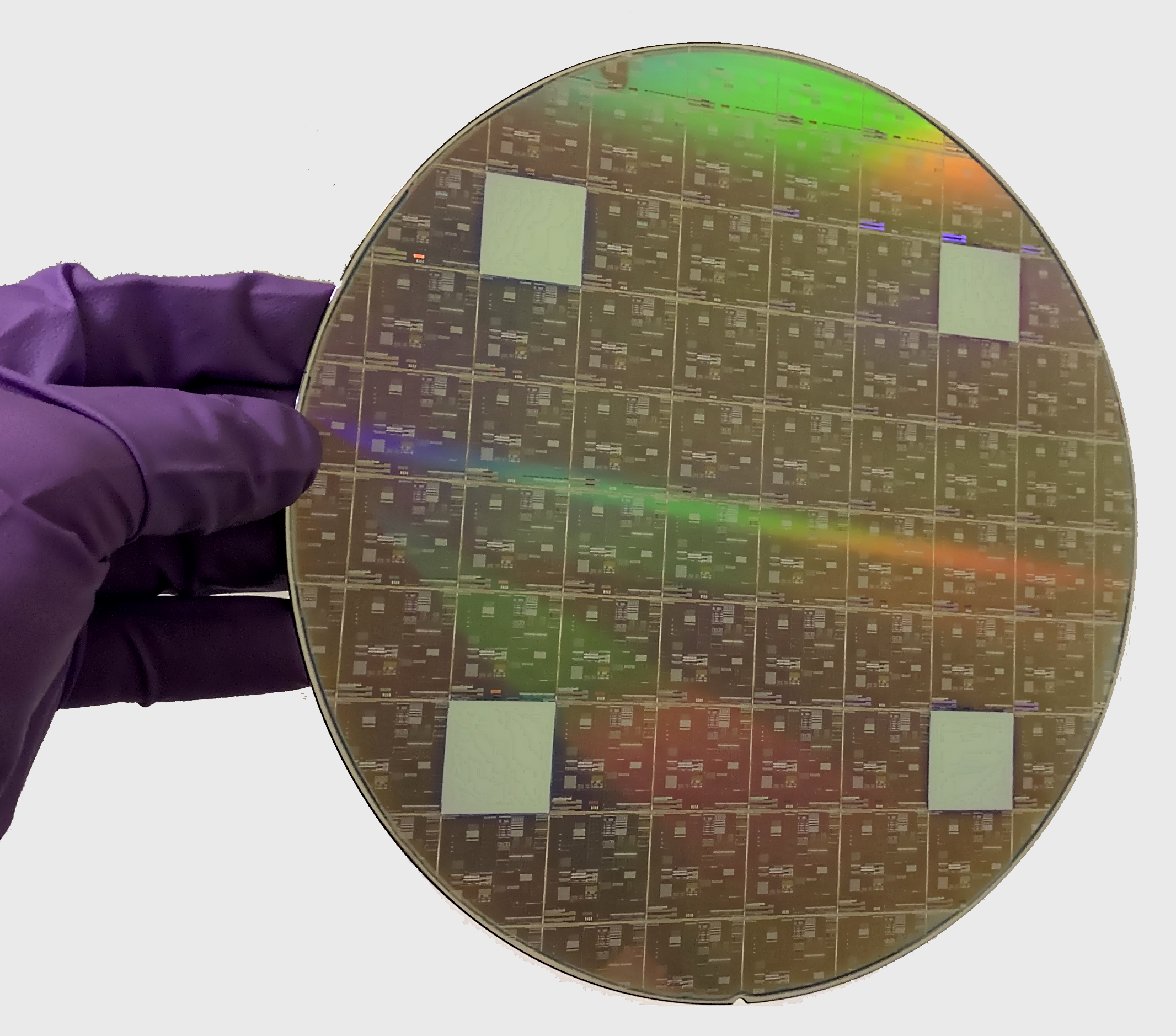
A Purdue team has fabricated more than 100,000 indium-oxide transistor devices in three vertically stacked tiers on 200-mm silicon wafers. It also connected devices across tiers into working memory and logic circuits, a step toward putting different chip functions in the same footprint.
Monolithic 3D integration builds new device layers directly on a wafer, rather than stacking separately manufactured dies. The challenge is adding those layers without overheating or damaging the electronics below. The researchers used atomic-layer deposition to form indium-oxide channels at about 225°C, within the low thermal budget used for back-end chip processing.
The fabricated stack combined ferroelectric transistors, which can retain a programmed state, with two types of indium-oxide field-effect transistor. Across 52 wafer dies, the team measured more than 100,000 devices and demonstrated cross-tier inverters, nonvolatile memory and embedded DRAM cells. The paper reports that the upper-tier processes did not degrade the measured lower-tier devices.
A separate four-tier design explores the platform’s potential for AI. It stores static model weights in ferroelectric nonvolatile memory and dynamic values in embedded DRAM, with computing logic across the same vertical stack. This arrangement is intended to increase useful memory and logic capacity in a fixed footprint while reducing data movement. In the authors’ system-level evaluation, the design recorded 1.4× to 2.9× speedups for GPT-2 and BERT-small workloads against a planar baseline with the same footprint and memory mix. The four-tier accelerator was modeled, not fabricated.
The authors say larger hardware demonstrations are needed to validate the projected accelerator gains. Further scaling will also require control of unwanted electrical coupling between layers and heat transport.
Sources
- Nature Nanotechnology paper, published September 15, 2026.
- Full author manuscript on arXiv.
- Illustrative wafer photograph, not from the study: Goldenvu, Wikimedia Commons, Processed 200 mm Si Wafer, used unmodified under CC BY-SA 4.0.
