Belgian research institute imec has printed chip test patterns with a 22-nanometre pitch, the distance from the centre of one line to the next. The September 8 announcement describes a single-exposure process using a long-established type of light-sensitive coating.
Chipmakers print patterns onto a light-sensitive coating, then transfer them into the wafer by etching away selected material. Imec and its suppliers improved the chemistry of this familiar coating, called a chemically amplified resist, alongside the etching process.
The experiment used high-numerical-aperture extreme-ultraviolet lithography, or High NA EUV. Extreme-ultraviolet light is focused by mirrors; numerical aperture measures how much light those optics can collect and focus. A higher aperture allows the machine to print finer features.
The demonstrations included winding and forked lines, plus holes for connections between chip layers. Imec says the results could extend this resist technology to selected layers of future logic chips. It cited further improvements in yield, the share of usable structures, as a development goal.
Sources
- Imec's September 8, 2026 technical announcement, including patterning results and the reference to SPIE presentation 14272-8.
- ASML: lithography mirrors and numerical aperture, technical background.
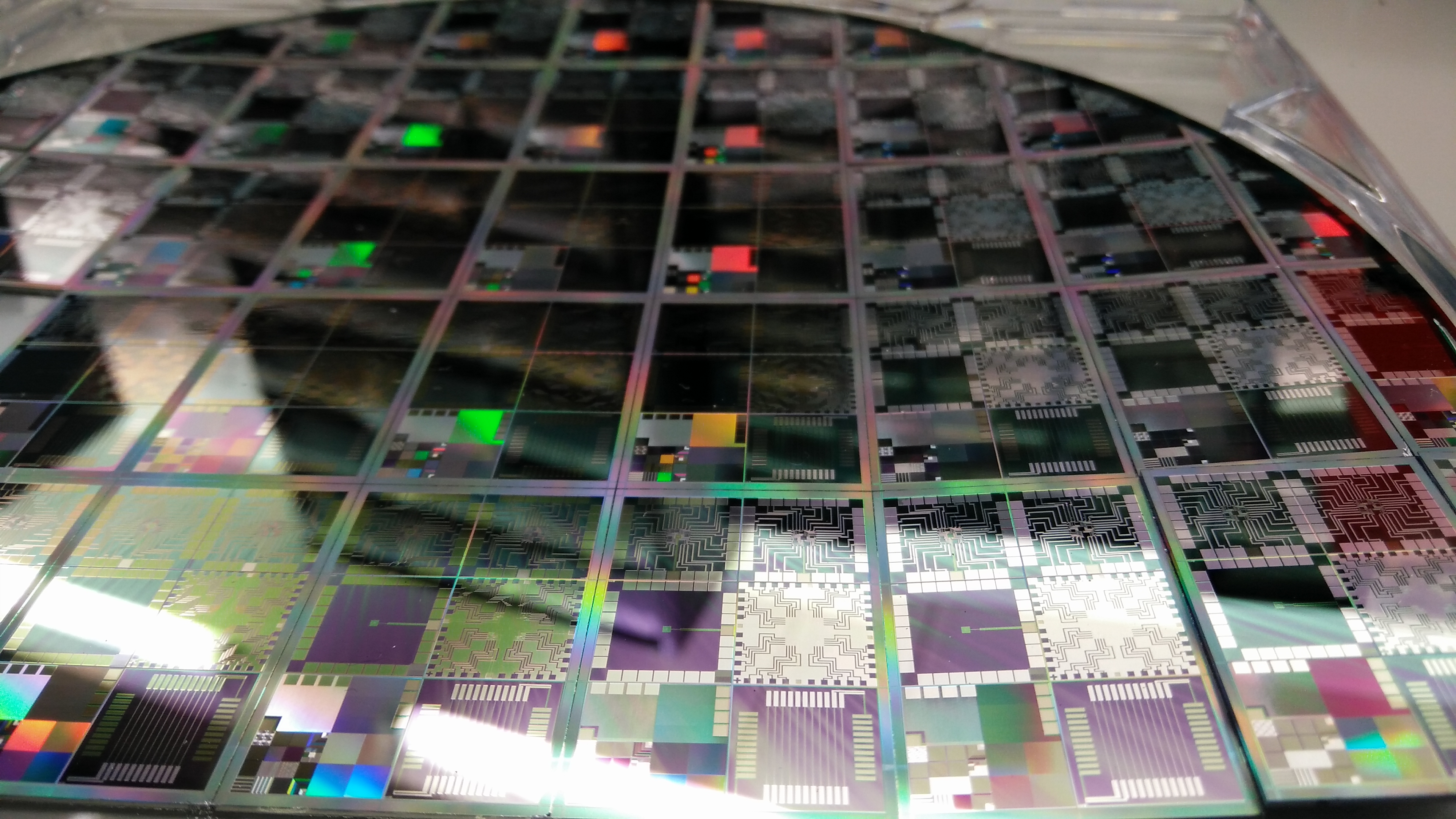
- Image: Semiconductor Wafer of Microelectronics, DrHughManning, January 26, 2017; CC BY-SA 4.0. Unaltered file photograph displayed at reduced size, not a photograph of the reported imec experiment.
